
- INTRODUCTION
The present photovoltaic (PV) market is dominated bycrystalline Si solar cells. Its cumulative level of capacityannounced in 2009 was 24 GW, and the European PVIndustry Association expects these announced capacitiesto grow by about 30% in 2010. Thereafter, the compoundannual growth rate will level off to about 20% during lateryears to exceed 65 GW in 2014 [1]. As can be seen, it isgenerally expected that the Si dominance in the PV marketwill continue for at least the next decade.
As published in the International Technology Roadmap for Photovoltaics (ITRPV) following the historicallearning curve as well as industry growth, the specificcosts per watt peak (Wp) of Si PV modules are expectedto decrease by 8–12% per year. According to the Crystalline Silicon PV Technology and Manufacturing (CTM)Group, this implies a more effective use of material, moreproductive manufacturing equipment and more advancedprocesses [2].
For the required cost reductions to be achieved, solarcell recombination losses at the rear side of the crystallineSi bulk material must be reduced using relevant industrialprocesses. The CTM Group estimates that a J0,rear below100 fA/cm2is needed after 2015.
A recently introduced dielectric for outstanding rearsurface passivation of p-type Si passivated emitter and rearcell (PERC)-type solar cells is Al2O3. Industrially relevantdeposition techniques for Al2O3 are thermal atomic layerdeposition (ALD) and plasma-enhanced chemical vapordeposition (PECVD) [3,4], and the underlying mechanismis based on chemical passivation—a low density of interface defects Dit—and field-effect passivation with a highdensity of fixed negative charges [5–12].
In this work, an approach is developed to integrate ALDAl2O3 as rear surface passivation for screen-printed large-areap-type Si PERC-type solar cells. First, a stack of Al2O3/SiOx/SiNxis developed to optimize the rear internal reflection; afterwhich the thermal stability of this Al2O3-based stack is investigated to improve its integration in PERC-type solar cells.
- EXPERIMENTAL
Saw-damaged, 1 Ω cm p-type solar grade Cz Si material is used for all minority carrier lifetime (teff) characterization. The Cz wafers are fifirst chemically etched in a NaOH : H2O solution and neutralized in a HCl : H2O mixture. Thereafter, an extra etching step in HF : HNO3 : acetic acid is performed. Finally, all Si wafer cleanings prior to Al2O3 deposition have a HF-last (Si-H) last step and fifinish with Marangoni drying [13]. Thermal ALD Al2O3 fifilms (≤10 nm) are grown at 200 C in a commercial ALD reactor (Savannah S200, Cambridge NanoTech, Cambridge, MA, USA) using trimethylaluminium and deionized water as precursors. SiOx and SiNx capping layers are deposited in a commercial PECVD system.
Screen-printed large-area p-type Si PERC-type solar cells are made following the process sequence listed in Table I. The cells are made using the same Cz Si solar grade material mentioned previously, are 150-mm thick and have a 60 Ω/sq emitter.
Table I. Baseline p-type Cz Si passivated emitter and rear cell (PERC)-type solar cells, having an (Al2O3)/SiOx /SiNx rear surface passivation stack. The 148.25-cm2 cells are 150-mm thick, have a base resistivity of 1 Ω cm and an emitter of 60 Ω/sq.
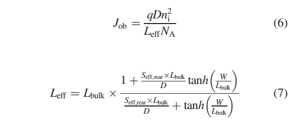
An approximation of J0,rear at low injection for the developed Al2O3 -based rear surface passivation stack is calculated using Equation (1), with acceptor density NA, intrinsic carrier concentration ni , elementary charge q and the effective rear surface recombination velocity Seff,rear. How Seff,rear is being calculated from the effective surface recombination velocity of the passivated area (Seff,pass) and effective surface recombination velocity of the metalized area (Seff,metal) is explained subsequently.

The Seff,pass is estimated from teff by applying a lifetime tester (Sinton WCT-100, Sinton Instruments, Boulder, CO, USA) and using Equation (2), with tbulk as the bulk lifetime and W as the c-Si wafer thickness. The tbulk is estimated by passivating various thicknesses of equivalent Cz Si material (700-mm-thick p-type CZ Si wafers are thinned down during the NaOH : H2O etching step). Hence, a plot of inverse effective lifetime as a function of inverse wafer thickness leads to an estimation of tbulk, which is the intercept of the linear fifit with the 1/teff-axis as can be seen from Equation (2). For the Si material used in this work, the tbulk is calculated to be 714 ± 76 ms at 1 1014/cm3 injection level.

The Seff,metal is estimated using quasi-steady-state photoconductance-calibrated photoluminescence (QSSPC-PL; BT Imaging, Surry Hills, NSW, Australia), which is needed to be able to measure the teff of samples that are partially laser ablated and metalized. Consequently, a plot of the Seff,rear as a function of metalized fraction (X) gives an estimation of Seff,metal that can be calculated from the slope of the linear fifit as shown by Equation (3). Varying the pitch of the local point contacts, the Seff,metal is estimated to be 1726± 74 cm/s for the Al sputtering used as rear metalization in this work.

Finally, the Seff,rear is calculated by employing Equation (4), with the Seff,pass estimated from measuring teff at 1 1014/cm3 injection level (using 714 ms as tbulk in Equation (2)), Seff,metal equal to 1726 cm/s, X equal to 0.0147 as typical laser ablated fraction in this work, Y is the blistering surface coverage as measured with optical microscopy and Z is the fraction of blistering contacted during co-fifiring, as explained in Section 3.2.

Using the ideal one-diode equation, the VOC is simulated starting from the Seff,rear, as explained subsequently. The VOC is obtained from the contribution of the emitter saturation current density Joe and the base saturation current density Job, as displayed in Equation (5).

The Joe is extracted from symmetrical device structures using QSSPC measurements, whereas the Job is obtained analytically according to Equation (6), with D as the diffusion coeffificient of minority carriers in the base and Leff as the effective diffusion length. This Leff is dependent on the Seff,rear, the bulk diffusion length Lbulk, the diffusion coeffificient D, and W as seen in Equation (7) [14].
The used current–voltage (I–V) setup is a steady-state Xe lamp solar simulator (WXS-200S-20, Wacom Electric Co., Saitama, Japan; AM 1.5 G) with an illuminated area of 200 200 mm2 , a small bias error and a good stability over time, as shown in [15].
- RESULTS AND DISCUSSION
3.1 Enhanced internal reflflection of the Al2O3-based rear surface passivation stack
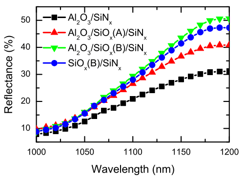
Figure 1 compares the reflflectance between 1000 and 1200 nm of PERC-type solar cells on p-type Cz Si substrates with alkaline-textured front surface and polished rear surface passivated by a stack of Al2O3 /SiNx , SiOx / SiNx or Al2O3 /SiOx /SiNx . For the SiOx layer, two thicknesses have been used, where SiOx (A) is thinner compared with SiOx (B). From these reflflectance measurements, it is clear that for optimal rear internal reflflection of an Al2O3 – based rear surface passivation, it has to be capped with a thick-enough SiOx layer and SiNx . These rear surface passivation stacks have been optimized in previous work (see [16] for more details).
This means that for optimal rear internal reflflection, the Al2O3 has to be capped with SiOx /SiNx before the co-fifiring step (Table I). As explained in [17], capping a thin ALD Al2O3 fifilm with SiOx and/or SiNx or annealing a stack of Al2O3 and SiOx and/or SiNx can lead to blister formation. Blistering is the partial delamination of an Al2O3-based stack caused by gaseous desorption in the Al2O3 layer upon thermal treatments above a critical temperature (typically 350 C for ALD Al2O3); the capped Al2O3 layer acts as a gas barrier and blister formation occurs. Blistering of Al2O3 and capped Al2O3 layers has been observed for various deposition techniques: thermal ALD [17], plasmaenhanced ALD [18] and PECVD [19,20]. Using a thinenough (≤10 nm) Al2O3 layer and performing an annealing step prior to capping are shown to be the solution to create blister-free Al2O3-based passivation stacks.
Figure 1. Reflflectance at high wavelength for passivated emitter and rear cell-type cells having a rear surface passivation stack as indicated. For the SiOx layer, two thicknesses have been used, where SiOx(A) is thinner compared with SiOx(B).
3.2. Thermal stability of the Al2O3-based rear surface passivation stack
Blister-free screen-printed large-area p-type Si PERC-type solar cells are made as indicated in Table I, using an “out gassing” thermal treatment for 20 min in N2 after the Al2O3 deposition and prior to the SiOx /SiNx capping. Figure 2(a) shows the VOC of these cells as a function of the out-gassing temperature. Also the blistering surface coverage for the Al2O3 /SiOx /SiNx stack is shown, as measured by optical microscopy. As a reference, the VOC of SiOx /SiNx -passivated PERC is also given. Figure 2(b) gives the Seff,rear as calculated using Equation (4), with Y as the blistering surface coverage shown in Figure 2(a) and Z as the fraction of blistering contacted during co-fifiring. Using the simulation approach explained in the aforementioned experimental part, the VOC depicted in Figure 2(c) is simulated from the Seff,rear values shown in Figure 2(b). The Seff,rear and VOC in Figure 2(b) and (c) are calculated as a function of out-gassing temperature as well.
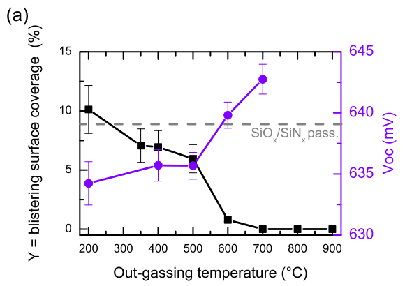
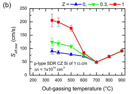
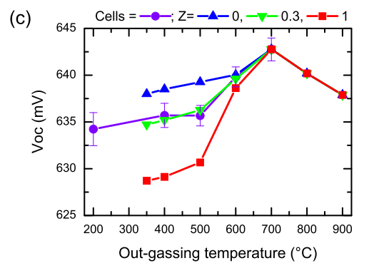
Figure 2. (a) Total blistered area and average VOC for Al2O3/SiOx/ SiNx rear passivated p-type Cz Si passivated emitter and rear celltype solar cells. The 10-nm Al2O3 layer has been out-gassed before the SiOx/SiNx capping by using temperatures shown on the horizontal axis. (b) Calculated Seff,rear as a function of out-gassing temperature. Seff,rear is estimated using Equation (4) and the blistering surface coverage shown in (a) as Y. (c) Simulated VOC using the Seff,rear depicted in (b) and the ideal one-diode equation (Equation (5)). Also the average measured VOC is shown.
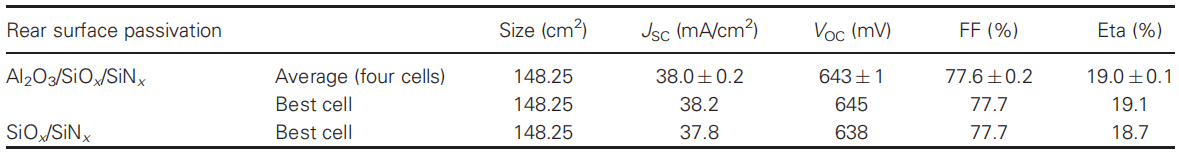
Table II. Overview of the cell characterization results (AM 1.5 G) for the 148.25-cm2 (Al2O3)/SiOx/SiNx passivated p-type Cz Si PERC-type solar cells. The processing sequence is given in Table I. The cells are 150-mm thick and have a base resistivity of 1 Ω cm.
As can be seen in Figure 2(a), the average VOC of the Al2O3/SiOx /SiNx -passivated PERC-type cells clearly improves as a function of out-gassing temperature. Even more, after out-gassing at 600–700 C, the Al2O3/SiOx / SiNx passivated cells are clearly better passivated at the rear compared with the SiOx /SiNx passivated cells. Together with this improvement in VOC, there is an obvious decrease in blistering as a function of out-gassing temperature. Applying this fraction of blistering and a factor Z for the probability of contacting through a blister during co-fifiring in Equation (4), an estimation of Seff,rear is obtained. Simulating the expected VOC using this Seff,rear, it is very clear that the increase in measured VOC as a function of out-gassing temperature is directly linked to the decrease in blistering. If the out-gassing temperature is too low during co-fifiring, about 30% of the blisters become local point contacts; hence, the Seff,rear increases and consequently the VOC decreases. For out-gassing temperatures above 800° C, the Seff,rear starts to increase again.
3.3. Integration of Al2O3/SiOx/SiNx as rear surface passivation for p-type Si PERC
The average and best cell results for the Al2O3 /SiOx /SiNx – passivated PERC-type solar cells out-gassed at 700 C after the Al2O3 and prior to the SiOx /SiNx deposition steps are listed in Table II. Also the best reference SiOx /SiNx -passivated PERC-type solar cell result is given. The internal quantum effificiency (IQE) at high wavelength is shown for both SiOx /SiNx and Al2O3 /SiOx /SiNx passivated cells in Figure 3. Figure 4 provides the cell characteristics for one of the Al2O3 /SiOx /SiNx passivated solar cells as have been independently confifirmed by FhG-ISE CalLab.
As seen in Table II, for Al2O3/SiOx /SiNx -passivated PERC-type solar cells, an optimum reaching an average cell effificiency of 19.0% is found and independently confifirmed by FhG-ISE CalLab (Figure 4), as compared with 18.7% for the best SiOx /SiNx -passivated solar cell. There is an obvious gain in VOC and JSC of 5 mV and 0.2 mA/cm2 , respectively, thanks to enhanced rear surface passivation and rear internal reflflection. This improved Al2O3 /SiOx /SiNx rear surface passivation is also confifirmed by the IQE measurements at wavelengths between 1000 and 1200 nm as shown in Figure 3. Using Equation (1), from the minimal Seff,rear depicted in Figure 2(b), a J0,rear of 92 ± 6 fA/cm2 is approximated for the Al2O3/SiOx /SiNx rear surface passivation, well in line with the ITRPV roadmap beyond 2015 [2].
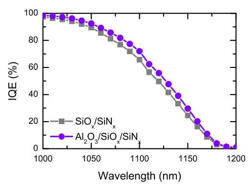
Figure 3. Internal quantum effificiency (IQE) at high wavelength for p-type Cz Si passivated emitter and rear cell-type solar cells, comparing the Al2O3/SiOx/SiNx and SiOx/SiNx rear surface passivation stacks.
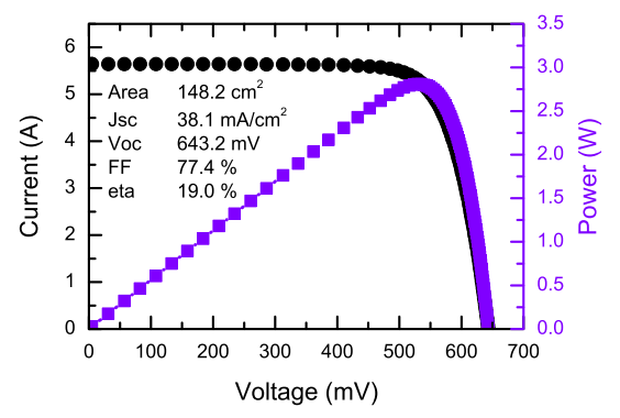
Figure 4. Current and power as a function of voltage for one of the Al2O3/SiOx/SiNx-passivated cells (Table II), as independently confifirmed by FhG-ISE CalLab.
- CONCLUSIONS
In this work, an Al2O3/SiOx /SiNx rear surface passivation stack is developed for screen-printed large-area p-type Si PERC-type solar cells. An average cell effificiency of 19.0% is reached and independently confifirmed by FhG ISE CalLab. Compared with SiOx /SiNx -passivated cells, there is an obvious gain in VOC and JSC of 5 mV and 0.2 mA/cm2 , respectively, thanks to improved rear surface passivation and rear internal reflflection.