
1 INTRODUCTION
Silicon solar cells with full-area screen-printed Al-BSF currently dominate the commercial market because of low cost and process simplicity. These cells are limited in terms of efficiency due to a high rear surface recombination velocity (200-600 cm/s) [1, 2]. To overcome the efficiency limitations, passivated emitter and rear solar cells (PERC) with local Al rear contacts represent a very promising option for next-generation industrial solar cells as stated in the International Technology Roadmap [3]. An industrial PERC process flow typically involves wet chemical polishing of the textured rear surface [4]. Horzel et al. [5] reported that the conversion efficiency significantly improves with reduced rear surface roughness when applying a SiOx /SiNy rear surface passivation.
In this paper, we investigate the impact of the rear surface roughness on the surface recombination velocity and on the rear reflectance based on test wafers and PERC solar cells. We investigate the degree of polishing required for two different surface passivation layers, SiO2 /SiNx and Al2O3 /SiNx .
2 DEPENDENCE OF THE SURFACE RECOMBINATION VELOCITY ON THE REAR SURFACE ROUGHNESS BASED ON TEST WAFERS
In order to analyse the impact of the surface roughness on the surface recombination velocity, we use 300 µm thick p-type boron-doped FZ wafers. After wafer cleaning and double sided alkaline texturing, we subsequently polish both sides of the FZ wafer using the RENA InPolish tool at ISFH. We vary the polishing time of the single sided wet chemical polishing process resulting in different silicon removals between 0 and 20 µm in order to obtain different surface roughness ranging from textured to planar. We compare two different passivation layer stacks. Either a stack of thermal SiO2 (10 nm thickness) and PECVD SiNx or alternatively atomic layer deposited (ALD) Al2O3 (10 nm thickness) with a PECVD SiNx capping layer. Finally, the wafers are fired in a conveyor belt furnace with a typical firing temperature profile. Afterwards, we measure the carrier lifetime by dynamic ILM [6, 7]. We prepare a second set of wafers where we locally open the rear passivation by laser contact openings (LCO) and then apply a full-area Al screen printing. After firing, we measure the lifetime by dynamic ILM. This methodology allows to determine the surface recombination velocity of the passivated areas Spass and the surface recombination velocity of the metallised areas Smet [8].As a reference we process wafers without texturing and wet chemical polishing. Thus the passivation layer is deposited directly after cleaning and damage etching on the FZ wafer. The surfaces of these wafers are termed planar.
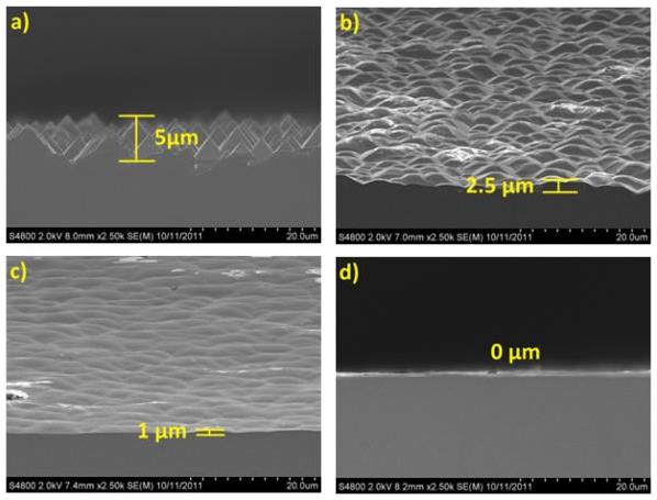
Figure 1: SEM x-section images of different polishing removals: a) textured b) 5.8 µm c) 14.0 µm d) 20.9 µm. Derived from the SEM images, the average surface roughness is around 5 µm, 2.5 µm, 1µm and 0µm, respectively.
Figure 1 shows scanning electron microscope (SEM) cross sections of alkaline textured wafers with varying wet chemical polishing times resulting in different Si removals between 0 µm and 20.3 µm. The resulting surface roughness varies between 0 µm (20.9 µm removal) and 5 µm (0 µm removal, fully textured).
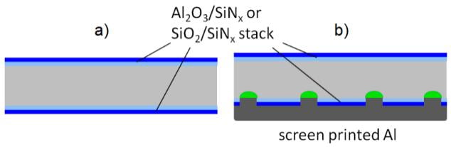
Figure 2: Schematic drawing of FZ wafers for lifetime measurements. Symmetrical test wafers of type a) are used to determine the surface recombination velocity (SRV) Spass. Wafers with rear metallization (type b) allow for determining the SRV in the passivated (Spass) as well as the metallised (Smet) areas.
Figure 2 shows schematic drawings of the test wafers resulting from the process flow as described above.
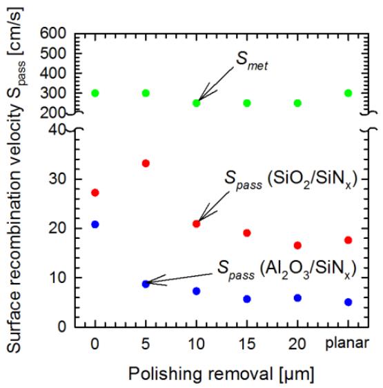
From the measured lifetimes on fully passivated wafers we calculate the upper limit of surface recombination velocities Spass = W/2*τeff as shown in Fig. 3. For SiO2 /SiNx passivation stacks, we observe a decrease from about 30 cm/s for textured wafers to values below 20 cm/s for the planar case. In contrast, the Spass values of Al2O3 /SiNx improve to below 10 cm/s already for small polishing removals of 5 µm. Fig. 3 shows the results for partly metallised and partly Al2O3 /SiNx passivated wafers according to Figure 2b). The SRV of the local screen-printed Al contacts, Smet, is independent of the rear surface roughness and remains constant at values around 300 cm/s. This result is confirmed by SEM cross sections which show that the Al back surface field (BSF) thickness is independent of the polishing removal. The SRV at passivated areas Spass fits well to the results of fully passivated wafers and are therefore not explicitly shown.
Figure 3: Surface recombination velocities on SiO2 /SiNx and Al2O3 /SiNx passivated wafers for different Si polishing removals on the surface. Values for Smet are extracted from Al2O3 /SiNx passivated wafers.
3 IMPACT OF THE REAR SURFACE ROUGHNESS ON PERC SOLAR CELLS
In order to investigate the impact of the rear surface roughness on PERC solar cells, we develop a process flow where we systematically vary the rear surface roughness without influencing other process parameters. We use 190 µm thick p-type 156×156 mm² boron-doped Cz-silicon wafers. The process flows are shown in Fig. 4.
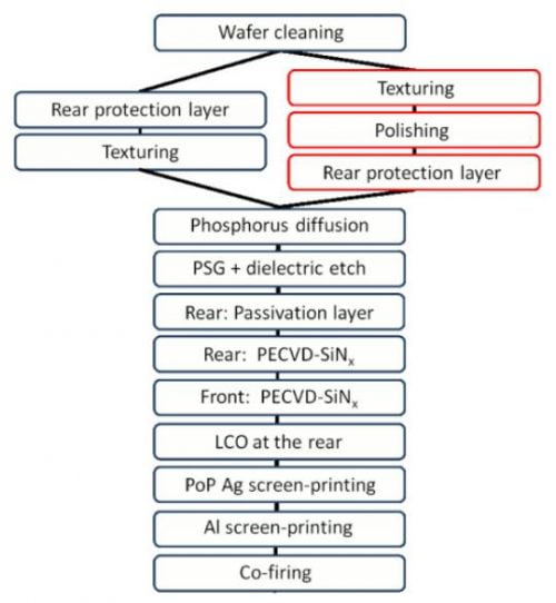
Figure 4: Process flows of the PERC solar cells. Reference PERC cells (blue) with planar rear side are compared to wet chemically polished cells (red) with different surface roughness.
The blue process flow refers to the reference PERC process flow applying a planar rear side [9]. The red process steps describe the modified process flow applying the wet chemical polishing process at the wafer rear after double sided texturing. We start PERC cell processing with wafer cleaning and a KOH damage etch. Aiming at a final wafer thickness of 150 µm the time of the KOH damage etch step is adjusted for the different rear side polishing removals. After texturing, the RENA InPolish tool is used to polish the rear surfaces of the wafers. Variation of polishing time results in different Si removals between 0 µm and 20.9 µm. Therefore, the surface roughness corresponds to those of the wafers shown in Fig. 1. Afterwards, a rear protection layer is applied in order to allow a front side phosphorus diffusion followed by a wet chemical etch which removes both, the PSG on the front and the protection layer on the rear. We then compare to different rear passivation stacks, thermal SiO2 /SiNx and ALD Al2O3 /SiNx . In case of the SiO2 /SiNx stack we oxidize the wafers resulting in a 10 nm thin thermal SiO2 on both wafer surfaces followed by a PECVD SiNx capping layer on the rear. In case of the Al2O3 /SiNx stack, we deposited a 10 nm thin plasma-assisted ALD Al2O3 layer on the wafer rear followed by a PECVD SiNx capping layer. Afterwards, we deposit a SiN antireflective coating on the front surface. Local line openings are then formed by LCO. Using a Print on Print (PoP) screen printing process, we obtain Ag front fingers with a width of 70 µm. The aluminium rear contact is formed by full area Al screen printing. After each screen printing step, the pastes are dried. The process flow is completed by a firing step in a conveyor belt furnace. A schematic drawing of the resulting PERC solar cell is shown in Fig. 5.
The measured IV parameters of the PERC solar cells in dependence of the polishing removal are shown in Fig. 6. The reference PERC cells with planar rear side are displayed as well. The conversion efficiency η of SiO2 /SiNx passivated cells shows a strong dependence of the rear surface roughness. Moving from a textured to a planar rear side we observe an increase from 18.0 % to 19.2 % which is primarily caused by a strong increase of the short circuit current Jsc. In contrast, Al2O3 /SiNx passivated cells reveal only slight variations in the efficiency η around 19.5% for different rear surface roughness. The best efficiency of 19.7% was achieved by using a polishing removal of 7.5 µm. Also, the Jsc shows only a small improvement with increasing polishing removal. With respect to the open circuit voltage Voc, applying polishing removals of 5-10 µm leads to improvements of about 5 mV for both, SiO2 /SiNx and Al2O3 /SiNx rear passivation. In terms of fill factor FF the two passivation layer stacks show a rather contrary behavior. While there seems to be an increase from 76.4% to 78.0 % with increasing polishing removal for SiO2 /SiNx , the fill factor decreases from 78.8 % to 77.1% for Al2O3 /SiNx . Further investigations have to prove if the FF variations are systematic or not.
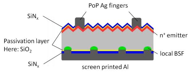
Figure 5: Schematic drawing of the SiO2 /SiNx rear-passivated PERC solar cell applied in this study. Note that in case of the Al2O3 /SiNx passivated PERC cells there is no thermal SiO2 between the emitter and the SiN AR coating.
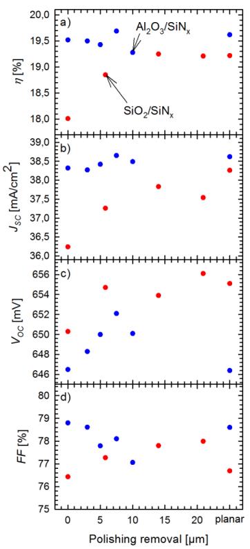
Figure 6: Conversion efficiency η (a), short circuit current JSC (b), open circuit voltage VOC (c) and fill factor FF (d) for Al2O3 /SiNx and SiO2 /SiNx passivated PERC solar cells with different rear polishing removals.
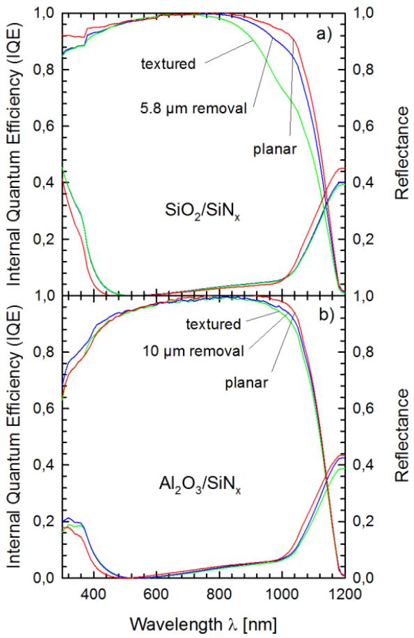
Figure 7: Internal quantum efficiency (IQE) and Reflectance for cells with SiO2 (a) and Al2O3 (b) passivation and rear surface roughness as indicated.
In order to analyse the impact of the rear surface roughness on the Jsc, we measure the internal quantum efficiency (IQE) and the reflectance for both passivation layers as shown in Figure 7 a) and b). The IQE in the infrared wavelength regime decreases with increasing rear surface roughness. For SiO2 /SiNx this decrease is much more severe than for Al2O3 /SiNx . The reflectance also slightly decreases with increasing surface roughness for both passivation layer stacks.
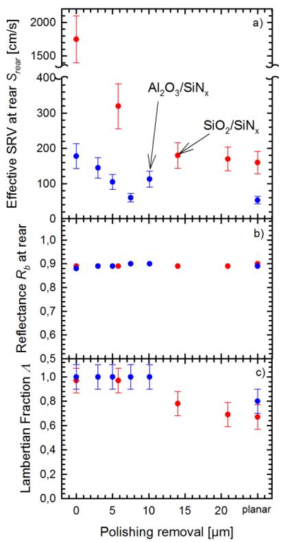
Figure 8: (a) shows the Srear values extracted from IQE measurements. (b) shows the reflectance of the rear surface Rb and (c) the Lambertian fraction Λ. All values are presented for Al2O3 /SiNx (blue) and SiO2 /SiNx (red) passivation and for different polishing removals.
Using the software Lassie from pv-tools, which is based on the analytical model for the QE introduced by [10], we analyze the reflectance and IQE to obtain the internal reflectance at the rear Rb , the Lambertian fraction Λ indicating the diffuse part of the rear reflectance and the effective rear surface recombination velocity Srear as presented in Fig. 8a. Rb is independent of the polishing removal with values around 0.9, whereas the diffuse part of the reflection Λ increases for rougher surfaces (see Fig. 8b and 8c). The rear SRV Srear of the SiO2 /SiNx passivated PERC cells strongly increases from about 160 cm/s for planar surfaces up to over 1750 cm/s for the textured rear whereas for Al2O3 /SiNx passivated PERC cells we only find a moderate increase of Srear with increasing surface roughness. The IQE analysis clearly shows that the advantage of Al2O3 /SiNx passivation results from electronic properties and not from optical ones.
4 CONCLUSION
The test wafer analysis shows that for both passivation layer stacks, SiO2 /SiNx and Al2O3 /SiNx , the surface recombination velocity (SRV) Spass reduces with increasing polishing removal which corresponds to a reduced surface roughness. However, in particular for small polishing removals of around 5 µm the Al2O3 /SiNx surface passivation achieves small SRV’s below 10 cm/s whereas the SiO2 /SiNx passivation shows Spass values around 30 cm/s. Accordingly, Al2O3 /SiNx passivation stacks are better suited to obtain low SRV’s and hence high PERC cell efficiencies for rough rear surfaces. The SRV of the local Al rear contacts Smet is independent of the surface roughness with values of around 300 cm/s. We develop a process flow for PERC cells which allows to analyse the impact of the rear surface roughness on PERC cells without influencing other process parameters. PERC solar cells with SiO2 /SiNx rear passivation show a strong increase of the conversion efficiency by up to 1.2% abs. with reduced rear surface roughness. In contrast, for Al2O3 /SiNx rear passivated PERC cells the rear surface roughness has a much smaller impact. The highest efficiency of 19.7% was achieved by applying a polishing removal of 7.5 µm. The internal quantum efficiency analysis reveals that the SiO2 /SiNx passivated PERC cells show a very strong increase of the rear SRV Srear with increasing rear surface roughness whereas the Srear of Al2O3 /SiNx passivated PERC cells achieves good values around 100 cm/s even for small polishing removals.